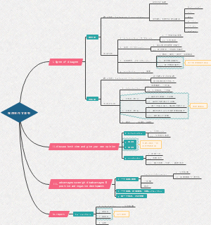
导图社区 1. Introduction and Overview of nanotechnology
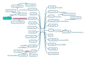
1. Introduction and Overview of nanotechnology
这是一篇关于1. Introduction and Overview o的思维导图,主要内容包括:Applications of Nanotechnology to Devices and Microsystems,Scaling Devices to Nanometer Range,Why Nanotechnology for Advanced Microelectronics and Bi
编辑于2024-09-14 16:29:28- 英文版
- 纳米技术
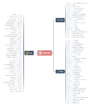
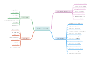
- 5. Etching
这是一篇关于5. Etching的思维导图,主要内容包括:Considerations for Dry Etching,Etch Rate Dependence,Dry Plasma Etching,Wet Chemical Etching,requirements and tradeoffs。
- 1. Introduction and Overview of nanotechnology
这是一篇关于1. Introduction and Overview o的思维导图,主要内容包括:Applications of Nanotechnology to Devices and Microsystems,Scaling Devices to Nanometer Range,Why Nanotechnology for Advanced Microelectronics and Bi
1. Introduction and Overview of nanotechnology
社区模板帮助中心,点此进入>>
- 5. Etching
这是一篇关于5. Etching的思维导图,主要内容包括:Considerations for Dry Etching,Etch Rate Dependence,Dry Plasma Etching,Wet Chemical Etching,requirements and tradeoffs。
- 1. Introduction and Overview of nanotechnology
这是一篇关于1. Introduction and Overview o的思维导图,主要内容包括:Applications of Nanotechnology to Devices and Microsystems,Scaling Devices to Nanometer Range,Why Nanotechnology for Advanced Microelectronics and Bi
- 相似推荐
- 大纲