导图社区 Lec3 E-beam lithography
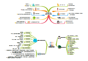
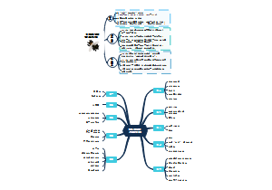
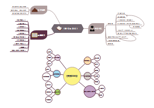
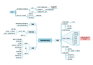
电子束光刻知识重点,整理了Electron beam lithography、Nano Imprint lithography 、Laser lithography、Extreme Ultraviolet lithography 的内容,喜欢的可以点个赞收藏一下哟~
社区模板帮助中心,点此进入>>
论语孔子简单思维导图
《傅雷家书》思维导图
《童年》读书笔记
《茶馆》思维导图
《朝花夕拾》篇目思维导图
《昆虫记》思维导图
《安徒生童话》思维导图
《鲁滨逊漂流记》读书笔记
《这样读书就够了》读书笔记
妈妈必读:一张0-1岁孩子认知发展的精确时间表
Lec3 E-beam lithography
E-beam lithography
用电子射线在sensitive to electrons的e-beam resist上画图案
精度很高,可以制造非常小的结构
merit
resolution
alignment accuracy
throughput
VS photo-lithography
E
low speed
point by point exposure
x diffraction limit (高solution)
$
更好的layer to layer alignment
x mask -> flexible
更好的depth of focus
P
high speed
parallel exposure
light d limit
photoresist 有更好的 etch resistance
resist profile
PMMA是一种electron resist,用其他两种试剂显影
气相沉积金属
e-beam exposure of resist
并不是一个一个点,而是会受到substrate的scattering
电子束能量越大,forward scattering 越小
e-beam registration这图啥意思啊不懂
marker scan 小方块 -> 用于get alignment 小于1nm
registration, markers, errors
几个marker 消除的错误类型
write time
子主题
typical writer column
spurce
tilt and shift control
blanking aperture
fast focus and stigmator coils
计算dose
base dose
but does depend on the process
方块算法
例子
光栅算法
一条细线,small line,会出现bias,意思是实际宽度总会大于设计的
细线算法
BSS:the w must always snap to an integral multiples of beam step size units.必须是步长的整数倍
所以如果w小于步长宽度,会被默认调整为步长宽度
线算法,还未仔细看
double Gaussian
pattern边沿dose增加When the double Gaussian is scanned along a line,
在两相邻pattern时会出问题,需注意extra effective dose in the centre of the pattern
dose需要根据pattern的不同而定
solid interaction
偏转
蒙特卡罗模拟,通常我们使用100keV的,得到的size会更准确
越deep,scattering的发生越明显
dose曝光能量 tests
确定最适的dose来clear out resist
用一系列doses来测试
resist
+:照到的去掉
-:照到的留下
pattern block fracture
影响resolution,line edge roughness,aliasing and discretization
Electron beam lithography
电子束光刻流程
1048576 (2^20 ) possible exposure positions of the beam in each axis.
fields & sub-fields
Main Field大正方形 (0.5 mm, 1 mm or 1.2 mm)可以有多个
回顾结构,pattern gen获取你的cad design
不明白啥意思,不是caddesign吗
到底是2还是3
避免重复曝光
proximity correction
边缘处提高dose,作为compensate
没明白什么叫中间的线会collapse
正胶清除负胶留
选择光刻胶厚度
30nm-3μm
3:1 for aspect ratio
高/宽
注意
subsequent etch or metallisation
金属层薄于resist
pattern resolution
pattern density
Nano Imprint lithography (NIL)
低成本高产量高分辨率
但必然产生上切profile
类型
也要涂胶匀胶;紫外固化胶
像沾了material再转移到新的基底上
加热加压融化
Laser lithography
利用激光的干涉,但实际上相当于光刻
Extreme Ultraviolet lithography (EUV)
for CPU,GPU
EUV motivation